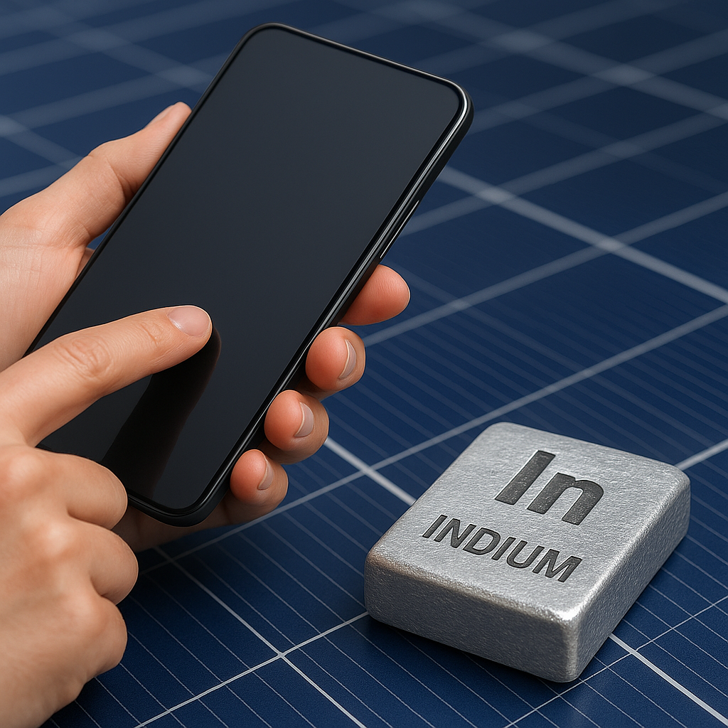
The metal indium plays a quietly dominant role in two of the 21st century’s most visible technologies: the screens we tap every day and the solar modules that promise cleaner energy. This article examines why indium has become indispensable for modern touchscreens and certain types of photovoltaics, how its unique physical and chemical properties enable those technologies, the supply and environmental challenges associated with its use, and the technical and policy pathways toward more resilient and sustainable deployment.
Fundamental properties that make indium indispensable
Indium is a relatively rare post‑transition metal with a combination of electronic and optical characteristics that make it ideal for transparent conductive films and thin‑film semiconductors. Chief among these is its role in the widely used indium tin oxide (ITO), a mixture of indium oxide and tin oxide that forms a transparent conducting oxide (TCO). ITO films combine high optical transparency in the visible spectrum with low electrical resistivity — a balance that is difficult to achieve with other materials.
Key practical properties:
- High carrier concentration and mobility when doped appropriately, enabling sheet resistances commonly below tens of ohms per square for devices while maintaining high visible transmittance.
- Good chemical stability and mechanical compatibility with glass and many polymer substrates, important for mass manufacturing of displays and solar cells.
- Processability: ITO can be deposited by sputtering and other scalable thin‑film techniques, which are already integrated into display and photovoltaic production lines.
The combination of these properties means that manufacturers can produce capacitive touchscreens that sense finger proximity and pressure reliably, while photovoltaic devices can extract and transport photogenerated charges efficiently through transparent electrodes without significantly blocking sunlight.
Indium in touchscreens: enabling modern human–machine interfaces
Capacitive touchscreens, which dominate smartphones, tablets, and many public displays, rely on a transparent electrode layer to detect changes in capacitance caused by a finger or stylus. The industry standard for decades has been ITO, whose combination of transparency and conductivity enables crisp displays with responsive touch sensing. ITO is typically deposited as a thin film (on the order of tens to hundreds of nanometers), providing the electrical pathways for touch controllers while allowing over 85–95% of visible light to pass through.
Beyond pure electrical performance, ITO’s compatibility with manufacturing is crucial. Sputtered ITO adheres well to glass substrates, can be patterned by photolithography or laser ablation to form touch sensors and electrode grids, and tolerates subsequent processing steps such as the deposition of organic layers, polarizers, or encapsulants. These practicalities have entrenched indium-based TCOs in display supply chains.
However, reliance on indium introduces vulnerabilities:
- Material cost volatility: Because indium is a byproduct of zinc and lead mining, its supply and price are sensitive to those primary industries and to concentration of production in select countries.
- Resource efficiency: ITO uses only small absolute quantities of indium per device, but the enormous scale of consumer electronics makes aggregate demand significant.
- Mechanical brittleness: ITO films are relatively brittle, which complicates flexible and foldable display designs and encourages research into alternative materials.
These challenges have driven research into alternatives such as aluminum‑doped zinc oxide (AZO), silver nanowire meshes, graphene and carbon nanotube films, and metal mesh electrodes. Alternatives can offer advantages — for example, metal nanowires or meshes can combine high conductivity with mechanical flexibility — but they face tradeoffs in durability, optical scattering, manufacturability, and cost. For the foreseeable future, ITO and therefore indium remain central to the mainstream touchscreen ecosystem.
Indium in photovoltaics: thin-film technologies and transparent contacts
In photovoltaics, indium appears in multiple roles. Most prominently, it is a constituent of CIGS (copper indium gallium selenide) thin-film solar cells, where indium is part of the absorber layer and contributes to the favorable bandgap and high optical absorption of the compound semiconductor. CIGS modules have achieved respectable module efficiencies in commercial production and research labs, and they benefit from lower material thickness and potential for flexible substrates.
Another significant role is as the transparent electrode: many solar cell architectures — including CdTe, perovskite, and tandem devices — employ TCOs like ITO or fluorine-doped tin oxide (FTO). In perovskite and other high‑efficiency cells, a transparent, low‑resistance top contact is vital to collect charge carriers without shading the absorber. Here, indium in the form of ITO provides that low‑loss, conductive window.
Performance impacts:
- CIGS absorber layers that incorporate indium enable tuning of the bandgap to better match the solar spectrum, improving cell efficiency.
- ITO as a top contact reduces series resistance and enables higher fill factors in thin‑film modules.
- In tandem and multi‑junction concepts, transparent electrodes must be nearly invisible optically while conductively robust — roles where indium‑based TCOs excel.
Nevertheless, the photovoltaic sector is also sensitive to indium availability and cost. Large‑scale deployment of indium‑rich PV technologies could pressure supply and encourage substitution or changes in module architecture to minimize indium content.
Supply, scarcity, and geopolitical considerations
Global indium production is modest in absolute terms compared with bulk metals. Because indium is mainly recovered as a byproduct of zinc (and sometimes lead or copper) refining, its supply depends partly on the economics and production levels of those primary metals. Key factors that influence indium availability include the concentration of refining capacity in specific countries, the economics of secondary recovery, and the pace of demand growth from displays and photovoltaics.
Concentration of supply can create geopolitical risks: when a small number of producers or refining centers dominate the market, export controls, regulatory changes, or trade tensions can cause price spikes and supply disruptions. These dynamics have repeatedly prompted manufacturers to explore alternative materials or to invest in supply chain diversification.
Because indium is not abundant and is often dispersed at low concentrations in ores, the material is effectively non‑renewable on a human timescale without significant improvements in recycling and urban mining.
Recycling, circular economy, and resource efficiency
Indium’s role in electronics makes end‑of‑life recycling an essential part of any strategy to secure supply. Recovering indium from display glass, LCD manufacturing waste, and discarded devices can reduce reliance on primary sources. Industrial processes for indium recovery include:
- Hydrometallurgical leaching of display glass followed by solvent extraction or ion exchange to separate indium.
- Thermal and chemical treatments of sputtering targets and manufacturing offcuts to reclaim indium compounds.
- Mechanical separation of e‑waste followed by chemical processing to extract indium from circuit boards and thin films.
Barriers to recycling include low concentrations of indium in large glass panels, mixed material streams that complicate separation, and the economic viability of recycling when primary indium prices are low. Policy measures (extended producer responsibility, recycling targets) and technical investments (improved sorting and chemical recovery) can help close the loop.
Alternatives and technical pathways to reduce indium dependence
Because of supply concerns and the push for flexible electronics, researchers and manufacturers pursue several complementary strategies to reduce indium demand:
- Material substitution: AZO (aluminum-doped zinc oxide), conductive polymers, silver nanowires, carbon‑based films, and emerging doped oxide chemistries can replace ITO in some applications. Each candidate has tradeoffs in conductivity, transparency, stability and cost.
- Device architecture: Minimizing TCO area, using metal grid lines to reduce required film conductivity, or employing patterned electrodes reduce the quantity of indium per device.
- Process optimization: Thinner ITO layers, improved deposition techniques, and higher material utilization in sputtering targets lower per‑unit indium use.
- Hybrid approaches: Combining a sparse metal mesh with a thin TCO layer can achieve performance while cutting indium content dramatically.
While progress is strong in lab settings, large-scale replacement of ITO is constrained by manufacturing inertia and the need for long-term stability and uniformity in high-volume production.
Environmental and health considerations
Mining and refining activities that yield indium can have environmental impacts typical of metal production — waste generation, energy use, and potential contamination if not properly managed. Because indium is often present in trace quantities, the environmental footprint per unit of recovered indium can be significant unless recovery is carefully optimized.
Worker exposure risks in mining and processing facilities necessitate occupational health safeguards; likewise, life‑cycle analyses of devices should account for upstream impacts of indium production and downstream benefits of recycling. Encouragingly, reuse and reclamation from manufacturing waste tends to yield high purities and lower environmental intensity than primary extraction.
Research trends and future prospects
Research directions that will shape indium’s role include:
- Higher‑efficiency photovoltaic devices that reduce area‑based material needs and thus lower per‑watt indium demand.
- Improved sustainable extraction and recycling technologies to increase secondary indium supplies.
- Development of scalable alternative electrodes that meet the performance, cost, and durability requirements of mass markets.
- Design for disassembly and modular electronics to facilitate material recovery at end of life.
Policy and market signals — such as strategic metal stockpiling, recycling mandates, and incentives for low‑indium technologies — will interact with technical advances to determine how quickly indium demand curves change. At present, indium remains a critical enabler of high‑performance displays and certain thin‑film photovoltaics, shaping both consumer experiences and renewable energy deployment.
Key takeaways for industry and policymakers
- Maintain investments in recycling to build a stable secondary supply and reduce environmental impacts.
- Support research into credible substitutes and hybrid electrode solutions to lower long‑term dependence on indium.
- Encourage industrial cooperation to improve material utilization and manufacturing yield, thereby reducing per‑device indium use.
- Monitor global supply chains and diversify sourcing to mitigate geopolitical risk tied to concentrated production.
Indium’s unique combination of optical and electronic properties has made it a foundational material for both interactive displays and advanced thin‑film solar cells. Finding balanced strategies — combining improved resource efficiency, smarter design, effective recycling, and responsible substitution — will be essential to keep the benefits of touchscreens and photovoltaics accessible, affordable, and environmentally responsible as demand grows.
