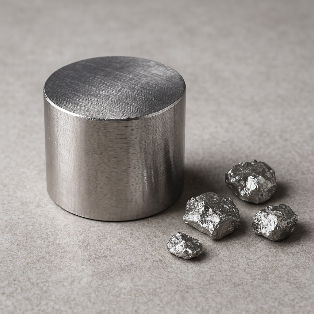
Indium is a soft, silvery post-transition metal with surprising importance far beyond its modest abundance. Though it exists only in trace amounts in the Earth’s crust, modern technology has elevated it to the status of a strategically important material. This article explores where indium is found, how it is produced and recycled, the many ways it is used in contemporary industry and science, and a selection of technical and historical facts that make indium a uniquely interesting element. Throughout the text, several key ideas are emphasized as they relate to both the opportunities and challenges associated with this remarkable metal.
Occurrence, Geology and Extraction
Indium is not typically mined as a primary ore; it is most often recovered as a byproduct of the processing of other metals, especially zinc. In nature it occurs in trace concentrations within sulfide minerals such as sphalerite (zinc sulfide), chalcopyrite, and galena, and in oxide minerals in minor amounts. Its average crustal abundance is on the order of 0.05 parts per million, which places it among the rarer metallic elements, yet it is sufficiently concentrated in some mineral-processing streams to be economically recovered.
Where indium is found
- Primary host ores: sphalerite (ZnS), chalcopyrite, and other polymetallic sulfides.
- Geographic production centers: historically, significant refined output has come from China, Japan, the Republic of Korea, Canada, Peru and Belgium, though global production varies with changes in base-metal mining and refining.
- Secondary sources: electronic waste and spent flat-panel displays are becoming increasingly important as potential recycling feedstocks.
Because indium is produced as a byproduct, its supply is strongly tied to the economics of base-metal mining and smelting rather than to indium-specific demand signals. This coupling can cause supply constraints and price volatility. Consequently, indium frequently appears on national “critical materials” lists and is the subject of strategic stockpiling and recovery efforts.
From ore to metal: extraction methods
Typical industrial routes for recovering indium involve:
- Concentration of base-metal ores and separation of zinc-lead residues;
- Hydrometallurgical treatment of flue dusts and residues from smelters to extract indium into solution;
- Solvent extraction and ion-exchange processes to purify indium from other dissolved metals;
- Electrolytic recovery or precipitation to produce metallic indium or indium compounds.
Advanced recycling processes target ITO-containing components and thin-film layers in displays and photovoltaic modules. Recovering indium from e-waste can be technically challenging because the metal is present in thin, adherent layers and often alloyed or mixed with glass and polymers, but successful recovery is a growing industry response to supply risk and environmental concerns.
Chemical and Physical Properties
On the periodic table, indium occupies group 13 with atomic number 49. It has a shiny, malleable appearance, and is soft enough to be cut with a knife at room temperature. Key properties include:
- Atomic number: 49
- Electron configuration: [Kr] 4d10 5s2 5p1
- Common oxidation state: +3 (though +1 compounds are known)
- Melting point: about 156.6 °C (low compared with many structural metals)
- Density: approximately 7.31 g/cm3 at ambient conditions
Indium forms a thin oxide layer in air, but unlike some other metals, its oxide does not strongly protect it from further reactions in all environments. It readily forms alloys with many metals (including lead, tin, silver, and bismuth), and some indium-based alloys have extremely low melting points that are useful in specialized soldering and fusible plugs. Indium’s ability to wet both metals and glass—and to remain ductile at low temperatures—gives it unique applications where other materials fail.
Isotopes and special nuclear properties
Natural indium consists primarily of two isotopes: 113In and 115In. The latter is technically radioactive but has an extremely long half-life, so for most practical considerations indium is treated as a stable element. Certain indium radioisotopes, such as Indium-111, are produced in cyclotrons and used in nuclear medicine as radiotracers and for diagnostic imaging.
Major Applications and Technological Roles
The modern importance of indium springs largely from its electrical and optical properties when combined into compounds and thin films. Several industrial sectors are highly dependent on indium for specific functions.
Transparent conductive films and displays
The most widely recognized application for indium is in indium tin oxide, commonly abbreviated as ITO. ITO is a transparent, conductive oxide used as a front contact in:
- Liquid crystal displays (LCDs)
- Touchscreens and capacitive sensors (hence the role in many smartphones and tablets)
- Organic light-emitting diode (OLED) displays
- Some solar cell technologies that require transparent electrodes
ITO’s combination of high optical transparency across the visible spectrum and relatively low electrical resistivity makes it difficult to replace. Deposition methods such as sputtering and evaporation are used to form thin ITO layers on glass or flexible polymer substrates. The demand for ITO has surged with the global deployment of touch-sensitive consumer electronics, making indium a critical component of everyday devices.
Semiconductors, photonics and LEDs
Several important semiconductor materials incorporate indium. Examples include:
- InP (indium phosphide) — used in high-speed and optoelectronic devices, including fiber-optic communications lasers and photodetectors.
- InGaN (indium gallium nitride) — an essential material for blue and green LEDs and high-brightness lighting; tuning the indium content allows control of emission wavelength.
- InAs and InSb — narrow-bandgap semiconductors used in infrared detectors and sensors.
These compounds underpin technologies ranging from long-distance optical communications to high-speed electronics and night-vision systems.
Photovoltaics
Thin-film photovoltaic technologies use indium in certain formulations. The copper indium gallium selenide family (CIGS) includes indium as a key element in efficient thin-film solar cells. CIGS cells can be deposited on flexible substrates and are known for relatively high efficiencies among thin films, though the use of indium in their absorbers raises concerns about resource availability as deployment scales.
Solders, thermal interfaces and cryogenics
Because of its low melting point and ability to remain ductile, indium is used in melt- or pressure-bonded joints and in thermal-interface materials where conformability is needed. Indium-based solders and bonding layers are used in sensitive electronics and in cryogenic applications where materials that maintain ductility at very low temperatures are required. It is also used as an adhesion layer in vacuum-tight seals between glass and metal.
Medical and nuclear uses
Medical radioisotopes such as indium-111 are used in nuclear medicine for imaging infection, tracking white blood cells, and other diagnostic procedures. Indium compounds are also used in experimental radiopharmaceuticals. In analytical chemistry, indium can serve as a carrier or tracer in certain contexts.
Supply, Recycling and Environmental Issues
Because mining of indium is tied to other base metals, its supply is vulnerable to shifts in mining practices and regional production changes. This has led to a growing emphasis on recycling—particularly from end-of-life displays, photovoltaic modules, and electronic scrap. Recovery processes aim to concentrate thin-film indium layers, dissolve and separate indium from glass and polymer matrices, and regenerate metallic indium or indium compounds suitable for reuse.
Challenges in recycling
- Thinness of indium coatings: ITO films are only tens to hundreds of nanometers thick, making mechanical separation difficult.
- Complex assemblies: displays combine indium-containing layers with plastics, adhesives and other metals.
- Economic tradeoffs: the small mass of indium per device means that collection, transport and processing must be aggregated to be cost-effective.
Nevertheless, advances in chemical recovery, thermal delamination, and mechanical processing are improving recovery rates. Industrial recycling not only reduces dependence on primary indium but also lowers the environmental footprint associated with extraction and refining.
Environmental and health considerations
Indium metal and many indium compounds have relatively low acute toxicity compared with heavy metals like lead or cadmium, but occupational exposure can have serious consequences. In recent decades, cases of severe lung disease, including pulmonary alveolar proteinosis and interstitial fibrosis, have been reported among workers in indium-tin oxide production facilities. These findings have prompted stricter workplace controls, exposure limits, and medical monitoring in industries that handle indium.
When discussing safety, it is important to distinguish between bulk indium metal and processed fine powders or aerosols of indium compounds, which present the highest inhalation risk. Proper ventilation, respiratory protection and process controls mitigate these hazards. Environmentally, indium is not known to bioaccumulate widely, but the localized release from mining and refining operations can contaminate soils and waters if not properly managed.
Economic and Strategic Considerations
Indium is often categorized as a critical raw material because of its combination of high technological importance and constrained supply. Factors affecting indium markets include:
- Demand growth from display manufacturing and photovoltaics;
- Concentration of refining capacity in a few countries;
- Technological substitutions, such as alternative transparent conductors (graphene, silver nanowires, doped zinc oxides) that could reduce ITO demand;
- Recycling rates and policies encouraging circular material flows.
The search for ITO substitutes is an active area of research driven by both material scarcity and performance goals. Alternatives such as aluminum-doped zinc oxide (AZO), fluorine-doped tin oxide (FTO), conductive polymers, carbon nanotubes, and graphene have shown promise for certain applications, but none has yet displaced ITO in mainstream high-volume display production. This is due to a combination of performance, scalability, and processing compatibility that ITO currently maintains.
Interesting Historical and Scientific Notes
The element was discovered in 1863 by Ferdinand Reich and Hieronymus Theodor Richter while they were analyzing zinc ores in Freiberg, Saxony. They observed spectral lines of a previously unknown element with a deep indigo-blue line, and the new metal was named from the Latin indium, meaning “indigo,” in reference to that spectral color. From a historical perspective, indium remained a chemical curiosity for many years before technological innovations in the 20th and 21st centuries made it indispensable.
Scientifically, indium’s role in compound semiconductors has been transformative. Its contribution to the development of bright blue LEDs via InGaN alloys, and its role in InP-based photonics for fiber-optic communications, underpin large swaths of modern information technology and lighting. The interplay between crystal chemistry, thin-film deposition techniques, and device engineering has made indium-containing materials central to multiple high-tech value chains.
Practical Tips and Future Directions
For industries that depend on indium, strategic measures include diversifying supply chains, investing in recycling infrastructure, and supporting research into alternative materials and device architectures that reduce indium intensity. For researchers and engineers, promising directions include:
- Improved recovery and recycling technologies for thin films and e-waste;
- High-performance ITO alternatives that match its conductivity, transparency and process compatibility;
- Optimization of thin-film deposition to minimize indium use while preserving device performance;
- Advanced occupational health controls and epidemiological research to limit adverse outcomes among workers.
From a materials-science perspective, indium will likely remain valuable for its unique combination of properties—conductive transparent oxides, low-melting alloys, and versatile compound semiconductors. Balancing its technological benefits with supply constraints and health considerations will shape how indium is used in the decades ahead.