The global digital economy runs on an intricate combination of materials, processes and logistics — and at the heart of that web are a number of often-overlooked elements. This article explores how rare metals underpin modern chips, the roles they play across fabrication, packaging and equipment, and why their availability shapes the resilience and innovation potential of the entire semiconductor industry. From the chemistry of compound semiconductors to the metallurgy of contacts and the economics of mining, understanding these materials clarifies both technical choices and strategic vulnerabilities.
The material foundations: where rare metals enter chip production
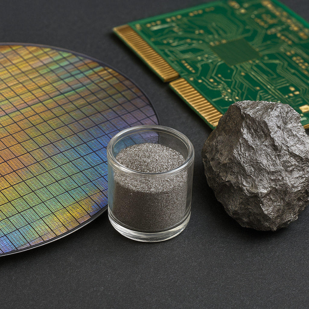
Semiconductor manufacturing is commonly associated with silicon wafers and photolithography, but many stages rely on specialized metals and compounds. Some elements are integral to the active device layers — for example, gallium and indium form compounds (GaAs, GaN, InP, InGaAs) used in high-frequency, optoelectronic and power applications. Others are essential in passive components and assembly: tantalum capacitors support stable power delivery on boards, while precious metals provide reliable electrical contacts and bonding.
Fabrication and device materials
- Compound semiconductors: III–V materials such as GaAs and GaN use gallium and indium to deliver properties impossible with silicon, including direct bandgaps for LEDs and lasers and high electron mobility for RF amplifiers.
- Doping and substrates: although dopants are often common elements (boron, phosphorus), advanced substrates and heterostructures may incorporate germanium or other specialty elements to improve performance.
- Thin films and coatings: noble metals and refractory metals (tungsten, molybdenum, platinum-group elements) are used as diffusion barriers, contact layers and hard masks during etch and deposition steps.
Packaging, interconnects and assembly
After wafer processing, chips are packaged and integrated with other electronics. Here, tantalum (in capacitors), indium (in solder alloys and thermal interfaces), and precious metals (gold and palladium in wire bonding and plating) are widely used. The mechanical and electrical reliability demanded by mobile devices, automotive systems and data centers means that small quantities of costly materials can be decisive for lifetime and performance.
Key rare metals: properties, uses and supply characteristics
Understanding a few representative elements clarifies how supply constraints propagate into technology planning. Below are several metals and groups that recurrently influence semiconductor design and manufacturing.
Gallium and Indium
Gallium and indium are central to III–V semiconductors and transparent conductive oxides (e.g., indium tin oxide, ITO) used in display drivers and touch panels. Their electronic and optical properties enable lasers, LEDs and high-speed transistors. Production is concentrated: gallium is primarily recovered as a by-product of aluminum and zinc refining, while indium comes mainly from zinc smelting. Limited primary mining, combined with by-product dependence, creates supply inflexibility and price sensitivity.
Tantalum and Niobium
tantalum excels in making capacitors with high capacitance per volume and excellent leakage characteristics — important in compact power supplies on IC substrates and printed circuit boards. Niobium shares some chemical properties and is sometimes considered as a substitute, but performance and processing differences restrict straightforward replacement at scale.
Precious and specialty metals
- Gold and palladium are used in bonding wires and surface finishes for corrosion resistance and reliable electrical contact.
- Platinum-group metals (PGMs) serve in specialty equipment, including sensors and catalyst-based cleaning or gas handling systems.
- Ruthenium and cobalt have emerged in certain interconnect and barrier-layer applications as feature sizes shrink and materials engineering becomes more complex.
Rare earths and related elements
While not typically inside logic chips, rare earth elements (neodymium, dysprosium, yttrium) support component subsystems: powerful magnets in motors for manufacturing tools and wafer handling, phosphors for inspection systems, and specialty alloys in equipment. These upstream uses make the broader electronics ecosystem sensitive to rare-earth availability.
Supply chain dynamics and geopolitical exposure
The economics of metals used in semiconductors differ from consumer commodities: volumes inside a single chip are tiny, but concentration of production and refining creates outsized systemic risk. A handful of countries host the majority of extraction or processing capacity for many critical elements. For example, historically large shares of rare earth processing have been in China, some indium and gallium refining is regionally concentrated, and cobalt extraction is geographically clustered with associated governance challenges. These patterns translate into price volatility and strategic friction.
Risk vectors
- Concentration of refining capacity — even if ore is mined elsewhere, the ability to produce high-purity metal for electronics often exists in few facilities.
- Trade restrictions and export controls — governments may limit shipments of precursor materials, affecting downstream device makers.
- Environmental and social governance (ESG) pressures — mining impacts, labor practices and permitting delays can reduce available supply.
Because the semiconductor industry depends on timely deliveries and ultra-high purity, disruptions that seem minor in bulk commodity markets can be crippling for fabs. Manufacturers therefore maintain strategic inventories, develop multi-sourcing strategies and participate in consortiums aimed at decoupling single points of failure.
Environmental impact, recycling and material circularity
Extracting and refining many specialty metals is energy- and chemical-intensive, producing significant environmental footprints. At the same time, recovering these metals from end-of-life electronics and industrial scrap — often called recycling or urban mining — offers an avenue to reduce dependence on primary mining and lower overall emissions. However, recycling semiconductors is technically and economically challenging due to tiny concentrations of valuable metals distributed across complex assemblies.
Barriers to effective recycling
- Material heterogeneity: chips are embedded in multi-layer packages, adhesives and substrates that complicate separation.
- Low per-unit concentrations: valuable metals are present in minute quantities per device, requiring economies of scale and specialized processing to justify recovery.
- Contamination and purity: semiconductors and related components demand exceptionally high purity; recycled streams must be refined carefully to meet specifications.
Despite these challenges, several pathways show promise: modular design for easier disassembly, selective chemical processes to extract target metals, and industry partnerships to aggregate scrap streams from datacenter operators and large-scale electronics recyclers. Policy instruments — subsidies for recycling plants, extended producer responsibility, and standards for material declarations — can accelerate the economics of circularity.
Technical innovation and substitution strategies
In response to supply risks and environmental concerns, engineers and materials scientists pursue substitution, material reduction and new device architectures. Examples include moving some interconnects back to copper where appropriate, developing silicon-based photonics to reduce dependence on compound semiconductors for certain optical functions, and exploring alternative capacitor chemistries that avoid scarce elements.
Trade-offs and limits of substitution
Substituting a metal is rarely trivial: performance, manufacturability, thermal stability and patent landscapes all matter. A material that works for a consumer device may fail in automotive or aerospace contexts where reliability thresholds are much higher. Consequently, the industry often invests in parallel approaches: short-term substitution where feasible and long-term material science to replicate or exceed the properties of critical elements.
Policy responses and corporate strategies
Governments and companies recognize that the micro-level choices of materials translate into macro vulnerabilities. Policy responses include stockpiling essential elements, funding domestic refining capabilities, enforcing supply-chain transparency and incentivizing research into alternatives. Corporations, for their part, invest in diversified sourcing, long-term offtake agreements with miners, qualification of secondary sources and participation in multi-stakeholder initiatives to improve mining governance.
Industry practices to mitigate risk
- Strategic inventory buffers calibrated to lead times and geopolitical risk assessments.
- Dual-sourcing and qualification of alternative suppliers to avoid single points of failure.
- Collaborative R&D consortia that pursue supply chain resilience through material innovation and recycling technologies.
Emerging trends and the path ahead
Looking forward, several intersecting trends will shape how rare metals continue to influence the semiconductor sector. Rising demand for power electronics, 5G/6G infrastructure, electric vehicles and AI accelerators increases consumption of specialty compounds and packaging materials. At the same time, advances in materials engineering — such as atomic-layer control, new alloy chemistries, and better recovery processes — can reduce dependence on the scarcest inputs. The net effect will depend on policy choices, investment in domestic and allied refining capacity, and the pace of technological substitution.
For engineers, policy makers and procurement teams in the semiconductor ecosystem, a realistic posture balances three elements: securing near-term supplies through risk-aware sourcing, investing in recycling and circular design to lower long-term exposure, and funding material science that delivers high-performance alternatives. Those who navigate this triad effectively will better align innovation cycles with the finite realities of the global materials base.
